8085 Microprocessor Architecture, Features, and Pin Diagram
Introduction
Intel 8085 is an 8-bit microprocessor introduced by Intel in 1976. It is a modified version of the Intel 8080 with two extra instructions (RIM & SIM). It is a 40-pin integrated circuit and its operating frequencies are 3,5 and 6 MHz. 8085 uses a single +5-V (Volt) Power Supply. It has a 16-bit address bus.
Configuration of 8085 Microprocessor
| Sr# | Parameters | Description |
|---|---|---|
| 1 | Data Bus Width | 8 bits |
| 2 | Address Bus Width | 16 bits |
| 3 | Program Counter (PC) | 16 bits |
| 4 | Stack Pointer(SP) | 16 bits |
| 5 | Registers | Accumulator, B, C, D, E, H,L, and Flag Register |
| 6 | Clock Speed | 3.2 MHz(single segment CLK) |
| 7 | Instruction Set | Accumulator, B, C, D, E, H, L, and Flag Register |
| 8 | Power Supply Voltage | +5 V DC |
8085 Microprocessor Architecture and Functions
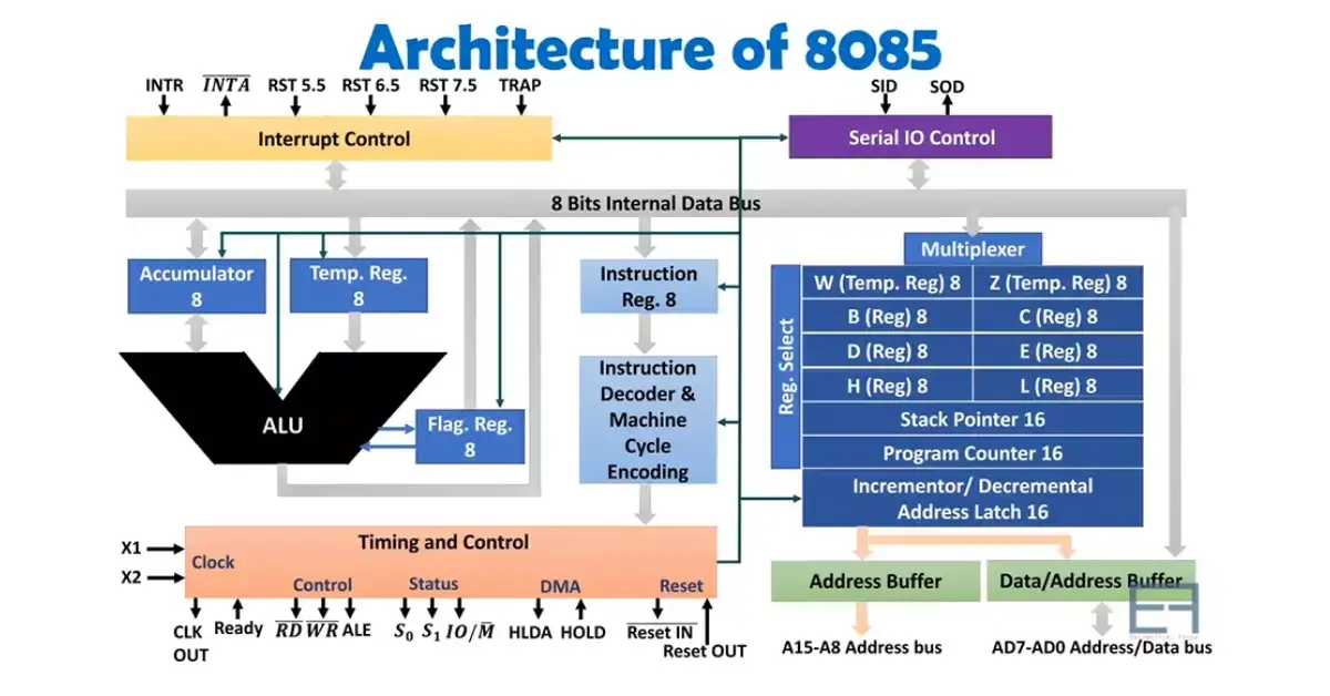
1. ALU(Arithmetic Logic Unit)
It is a logic circuit that is responsible for performing all the arithmetic and logical operations. The ALU receives the inputs from the Accumulator, Temporary registers and also stores results into the accumulator. The ALU accesses the flag register to set or reset the individual flags according to the result it has computed.
2. Serial Input/Output Control
A serial input/ output device consists of two pins eg SID and SOD.here SID means Serial input data and SOD means Serial output data. SID is used to read the bits serially, while SOD is used to send data serially bit-by-bit. They are used for serial communication between 8085 and Serial devices.
3. Interrupt Control
When an interrupt comes on one of the pins, 8085 suspends the current activity, saves the status, and jumps to a specific address where ISR (Interrupt service routine) is written. There are five interrupts in 8085 as clear in the above diagram. From right to left these are Trap, RST7.5, RST6.5, RST5.5, and INTR respectively. The importance of this sequence is that the priority of Trap is high and the priority of INTR is low. Trap, RST7.5, RST6.5, RST5.5 are vectored and INTR is non-vectored.
4. The Address and Data Buses
The address bus has 8 signal lines A8-A15 which are unidirectional. The other 8 address bits are multiplexed(time shared) with the 8 data bits. so the bits AD0-AD7 are bi-directional and serve as A0-A7 and D0-D7 at the same time. during the execution of the instruction, these lines carry the address bits during the early part, then during the late parts of the execution, they carry the 8 data bits. This whole process is known as the Demultiplexing of address and data bus.
5. Instructions Set
In 8085 Microprocessor Architecture, the instructions set is nothing except the instructions codes that are used to achieve the exact tasks. The instructions set is classified into different types such as logical instructions, control, branching, arithmetic, and data transfer instructions.
6. Registers
Microprocessors have temporary data holding places called Registers. These memory areas maintain data, such as computer instructions, storage addresses, characters, and other data.
Types of Registers in 8085 Microprocessor
a. General Purpose Registers (GPR)
The general purpose registers are used during various ALU operations for storing data temporarily. These registers are not used to store any specific type of information; instead, operands as well as addresses are stored at the time of program execution. However, the operand and address information may not be of the same size. For example, in 8-bit microprocessors, the data is 8-bit whereas the address is 16-bit.
| Sr# | Accumulator | Flags |
|---|---|---|
| 1 | B | C |
| 2 | D | E |
| 3 | H | L |
B(8), C(8)D(8),E(8),H(8), L(8) are 8-bit general purpose registers. It can be used singly or can be used as 16-bit register pairs like BC, DE, and HL. H and L can be used as a data pointer (hold memory address).
b. Special Registers
The special functions registers or Special Registers are used to perform some specific tasks. some special registers are Accumulator, Stack Pointer, Flag Register, Program Counter, Temporary Register, Instruction Register, MAR, and MBR. All of them are explained below.
i. Accumulator
It is an 8-bit register that stores 8-bit data. It stores the result of an operation as well as 8-bit data during input/output transfer.it is usually represented by the symbol “A”. The size of the accumulator is the same as the word size of the microprocessors. It is responsible for the following key operations.
ii. Program Counter
A program counter is a register used to store the address of the instructions to be executed next in the sequence of operations. The execution of the program is initialized by loading the program counter by the address of the first instruction of the program. This register is used to control the sequencing of the execution of instructions. This register always holds the address of the next instruction. Since it holds an address, it must be 16-bits wide.
iii. Stack pointer
A stack is an array of registers organized in a LIFO (Last-In-First-Out manner). The top of the element is always indicated by a special purpose register called Stack Pointer(SP). The size of the Stack pointer is equal to the length of the address. The stack pointer is also a 16-bit register that is used to point into memory. The memory this register points to is a special area called the stack. The stack is an area of memory used to hold data that will be retrieved soon. The stack is usually accessed in a Last-In-First-Out (LIFO) fashion.
iv. Flag Register
Flag register is also an 8-bit register. It shows the status of the microprocessor before/after an operation. Some important flags are S(sign flag), Z(zero Flag), AC(Auxiliary Carry Flag), P(Parity Flag), and CY(Carry Flag).
i.Carry Flag
The carry flag(CY) is an overflow from the 8-bit addition; it acts as a “borrow” flag during subtraction.
ii. Sign Flag
The MSB(Most Significant Bit) of the accumulator after the arithmetic or logical operation is copied into the sign flag. The 1 in the sign flag indicates the result is negative and 0 in the sign flag indicates the result is positive.
iii. Parity Flag
The Parity Flag (P) indicates no of I’s in the result of arithmetic or logical instructions which is always stored in the accumulator. If the number of I’s are even in the accumulator then it is called even parity and the parity flag is set to 1.
iv. Auxiliary Flag
It is an important flag. It indicates an overflow from the 4-bit of the results like CY which overflows from bit-8. The auxiliary carry flag is generally used in BCD (Binary Code Decimal) operations.
v. Zero Flag
The zero flag (Z) is set to 1 when the result of arithmetic or logical instruction is zero.
Registers Not Accessible to the Programers
i. Memory Address Register
Memory address register(MAR) stores the address information to be communicated to the outside world. The stored information is temporary.
ii. Memory Buffer Register
The information(data) to be stored in the memory is temporarily stored in the memory buffer register(MBR). The data to be received from the memory is also temporarily stored in the MBR and then transferred to microprocessor GPRs.
iii. Instruction Register(8)
An instruction fetched from the memory is temporarily in the instruction register (IR) before its decoding. During the opcode fetch cycle, the 8-bit opcode of an instruction is transferred into the instruction register. The contents of the instruction register are received by the instruction decoder and it is decoded to find the meaning of the instruction. After decoding the instruction decoder directs the timing and control section to perform a sequence of events to complete the execution of the current instruction. This process is also called the fetch-decode cycle.
Vi. Temporary Register
The ALU section is provided with one or more temporary registers. These registers are used to store temporary results when ALU performs the arithmetic and logic operations. They hold operands or addresses that are part of an instruction.
7. Bus Structure in 8085/Buses in8085
Before going to discuss the bus structure in 8085!
Let’s define what a bus is. Buses are lines that are connected from 8085 to the memory input and output devices. Here are three categories of buses in the microprocessor address line, data line, and control line as well. So in terms of buses, we may call them the address bus, data bus, and control bus respectively.
8. Control Unit
In 8085 Microprocessor Architecture, the control unit is used to supply the signals to get the specific processes. In Microprocessors, the internal and external circuits are controlled by timing and control units. The main four classes of such units are as
Pin Diagram of 8085 Microprocessor Architecture
When we talk about the Pin diagram of 8085, then you should know there are 40 different pins. Some of them are explained below one by one.
Pin Diagram Functional Units
1. Power Supply
In the power supply, there are two pins one is Vcc and the second is Gnd(Ground). Vcc is connected with +5V supply concerning Grnd is a reference.
2. Clock Frequency
In clock frequency, there are also two pins X1 and X2. x1 and x2 terminals are connected with a crystal clock, so a crystal oscillator will generate clock signals over and inside microprocessor 8085 that clock frequency will be divided by two. So here to operate at 3MHz we should give a 6MHz clock crystal oscillator.
3. Clock Out Terminal
It is used to provide a clock to external peripherals which we interface with 8085. So this terminal is used to give the clock to peripherals.
4. Address Buses
8085 has 16 lines for the address bus. These lines are split into two segments: A15-A8 and AD7-AD0. Here A15-A8 holds a higher Byte of address and AD7-AD0 has address and data lines.
5. Data Bus
8085 has 8 lines for data bus AD7-AD0. In executing an instruction during the earlier part of the cycle these lines are address lines and in the later part of cycle, it holds the data bus.
6. ALE(Address Latch Enable)
It is a positive going pulse generated every time in a machine cycle. It is used to latch lower addresses from AD7-AD0. When it is zero it indicates data on AD7-AD0.
7.Control Signals(ALE, RD,WR, IO/m and S1)
i. RD( read bar)
It is an active low signal which indicates read operation to be performed by 8085 over data lines. This read operation may be there with memory or IO devices.
ii. WR( write bar)
It is an active low signal which indicates write operation to be performed by 8085 over data lines. This write operation may be there with memory or IO devices.
iii. IO/M(Input/Output or Memory)
If it is logic “1”, IO operations should be done by 8085. If it is logic “0”, Memory operations should be done by 8085.
iv. S0 and S1
These are status signals.
8. Reset and Ready Terminals
i. RESET IN
When it goes low, 8085 is getting reset, and PC=0000H (Program Counter). The buses are tristate during that.
ii. RESET OUT
It indicates that the MPU is being reset. It can be used to reset other devices.
iii. Ready
This signal is used to delay the microprocessor’s read or write cycles until a slow-responding peripheral is ready to send or receive data.
When it goes low 8085 will wait for an integer number of cycles until it goes high.
9. Serial Data Communication
There are two terminals SOD(Serial Out Data) and SID(Serial Input Data).
i. SID(Serial Input Data)
It is used for serial data input.
ii. SOD(Serial Out Data)
It is used for serial data output.
10. 8085 Interrupts
i. INTR-Interrupt request
It is used for general-purpose interruptions.
ii. INTA-Interrupt Acknowledge
It is used for interrupt acknowledgment.
iii. RST7.5, RST6.5, RST5.5
These are vectored interrupts that transfer program control to specific memory locations. They have higher priorities than the INTR interrupt.
iv. TRAP
It is a non-maskable interrupt. It has the highest priority.
11. DMA Signals
These terminals are used for faster data exchange between memory and Input/output peripherals.
i. HOLD
This signal indicates that a peripheral such as the DMA controller is requesting the use of the address and data bus.
ii. HLDA
It is held to acknowledge and it is giving acknowledgement to hold a signal of DMA.
Machine Cycles in 8085 Microprocessor Architecture
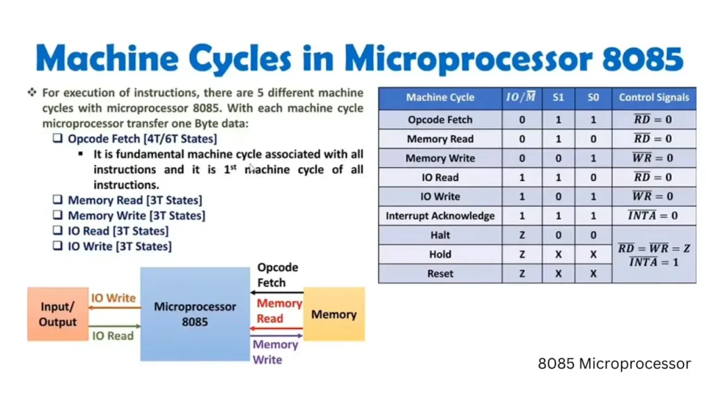
The execution of instructions is done by the 8085 Microprocessor by dividing each instruction into a sequence of Machine Cycles. There are five different Machine Cycles in 8085 Microprocessors. In each Machine Cycle Microprocessor transfers one byte of data. Some Machine cycles are explained below one by one.
| Sr# | Machine Cycle | IO/M | S1 | S0 | Control Signals |
|---|---|---|---|---|---|
| 1 | Opcode Fetch | 0 | 1 | 1 | RD=0 |
| 2 | Memory Read | 0 | 1 | 0 | RD=0 |
| 3 | Memory Write | 0 | 0 | 1 | WR=0 |
| 4 | IO Read | 1 | 1 | 0 | RD=0 |
| 5 | IO Write | 1 | 0 | 1 | WR=0 |
| 6 | Interrupt Acknowledge | 1 | 1 | 1 | INTA=0 |
| 7 | Halt | z | 0 | 0 | RD=WR=Z INTA=1 |
| 8 | Hold | z | x | x | = |
| 9 | Reset | z | x | x | = |
i. Opcode Fetch
In machine cycles, the Opcode Fetch is a Fundamental Machine Cycle which is associated with all the instructions and it is the 1st Machine Cycle of all instructions. In this cycle Microprocessor the instruction from memory and the Program counter accesses the memory location that contains the opcode. Then this instruction is transferred to the instruction register.
ii. Memory Read Machine Cycle
In this cycle, the data is being read from the memory.
iii. Memory Write
In this Machine Cycle, the Microprocessor writes the data to the specific memory location and it is also stored in the specific memory location.
iv. IO Read/IO Write
The last machine cycle of the Microprocessor is the Input/Output read or write cycle. Here the data is being transferred between Microprocessor and I/O devices.
Timing Diagram of 8085 Microprocessor
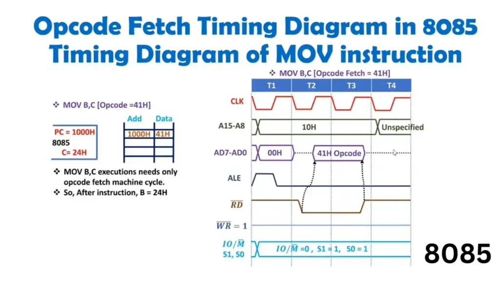
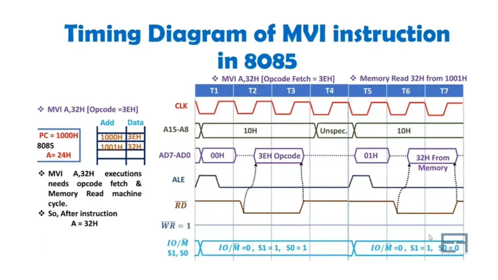
In the 8085 Microprocessor Architecture, the timing diagram helps to understand the performance and operations of Microprocessors. With the help of a timing diagram, we can clearly understand the functionality of the system and deep functional analysis of each instruction and execution. It is a graphical portrayal of instructions that signifies the period, data bus, clock cycle, and operation types. Some of the main timing diagrams are given below.
Timing Diagram of MOV Instruction
Timing Diagram of MVI Instruction
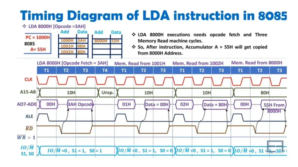
Timing Diagram of LDA Instruction
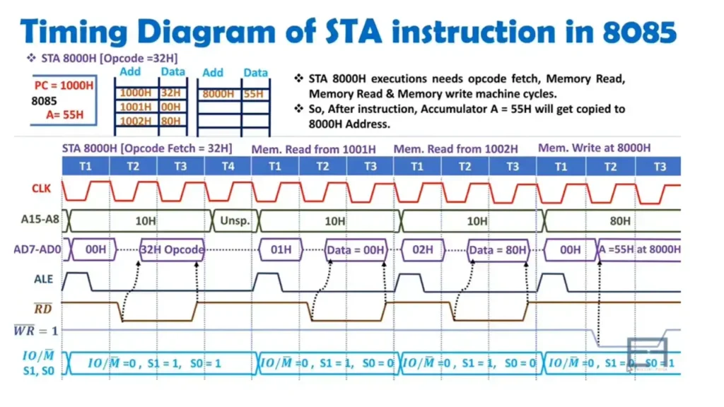
Timing Diagram of STA Instruction
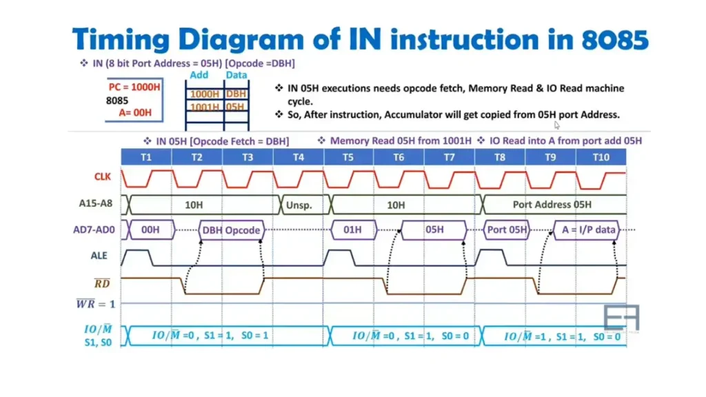
Timing Diagram of IN Instruction
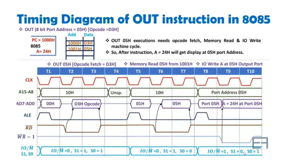
Timing Diagram of OUT Instruction
Features of 8085 Microprocessor
| Sr# | Feature | Description |
|---|---|---|
| 1 | Memory Capacity | 2^16=64 KB |
| 2 | Chip Construction | Single NMOS chip 6200 transistors |
| 3 | Operational Codes and Instructions | 246 operational codes, 80 instructions |
| 4 | Input/Output Address Lines | 8-bit input/output address lines (ability to address 2^8-256 input/ output ports) |
| 5 | Package Type | 40-pin dual in-line Package(DIP) |
| 6 | Bus Sharing | Shares bus with DMA controller for transferring information between I/O and memory. |
| 7 | Interrupt Mechanism | Enhanced Interrupt handling mechanism |
| 8 | Multi-Chip Configuration | Can operate as a three-chip microcomputer using IC 8355 and IC 8155 circuits |
| 9 | Internal Clock Generator | yes |
| 10 | Clock Cycle Characteristics | Functions on a clock cycle with a duty cycle of 50% |
| 11 | Address Bus | 16 bits |
| 12 | Data Bus | 8 bits |
Applications of 8085 Microprocessor Architecture
The advancement as well as the development of microprocessor devices brought a big change in the lives of people in every aspect of life. We can observe the applications of Microprocessors in multiple industries. As such devices are cost-effective, have less weight and other related features, and enhance the usage of microprocessors.
Applications of 8085 Microprocessor architecture include engineering applications, electronics, communication, and medical domain, etc.

